What Advantages Does HDI PCB Offer For Complex Routing?
HDI PCB Offer
As the digital world is getting more and more complex hour by hour, the gadgets that are associated with it are getting drastically smaller. To make the best use of this trend, HDI PCB technology has been developed to enable more connectivity and functionality within a smaller space. It is a significant advancement in the field of PCB design and layout, offering many benefits, including better signal integrity and higher data transmission rates. This is especially important for applications such as mobile phones, tablet computers and portable electronics.
Typical multilayer circuit boards can use up to 8 layers, but with HDI the number of layers is often significantly reduced. Consequently, the board’s physical size is also reduced. HDI also offers much higher routing density, which means more connections can be made within the same space.
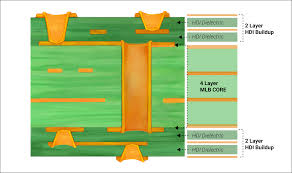
The main reason for this is that hdi pcb uses microvias, which are smaller than traditional vias and allow for greater routing density. Using these allows for a reduction in the number of layers needed for a given circuit, thus cutting down production costs and time to market. In addition, the smaller aspect ratio of the microvias also leads to improved reliability compared with standard vias.
What Advantages Does HDI PCB Offer For Complex Routing?
To achieve the required level of routing density, a combination of staggered and stacked microvias is used. Staggered microvias are placed with small offsets between layers, while stacked microvias are positioned on top of each other and on top of buried vias. This enables the signal to travel through more levels of vias in a shorter distance.
Another way in which HDI improves routing is through the use of a process called Via-in-Pad, in which the vias are placed directly on the flat pads of the copper layers. This makes it easier for the designer to route impedance controlled traces, as well as meet the fabricator’s DFM rules.
Besides improving routing density and simplifying the design and layout phases of electronic products, HDI also helps to reduce manufacturing costs by making the entire assembly process more efficient. This is due to the fact that there is a reduced amount of waste produced during fabrication, and the manufacturing process is also much faster.
The aerospace and defense industries require high-performance, lightweight PCBs for their sophisticated electronic systems. In order to meet these requirements, HDI PCBs have been developed to offer superior signal integrity and power distribution. This enables them to be used in various devices such as radar and navigation systems, flight simulators and military aircraft.
Although the advantages of HDI are clear, there are still some challenges that designers must face when designing with this technology. Achieving optimal component placement, routing, and signal integrity in a compact space requires special attention to detail and sophisticated design tools. However, with the right tools, it is possible to easily navigate these challenges and deliver a high-quality product that meets industry standards. Achieving this requires an understanding of signal integrity, thermal management, and manufacturability.















































Post Comment